REVOLUTIONIZING NANOTECHNOLOGY
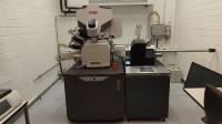
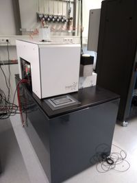
Introducing the Hybrid Dual Beam APT Microscope System ORBIS
Nanotechnology is a key technology for the development of various new products and materials. To be able to develop and produce these technologies or to ensure their quality, a special kind of microscopes is necessary. Atom probe tomography (APT) as well as dual beam microscopy (FIB/SEM) are powerful tools in nanotechnology with enormous scientific output. The combination of both techniques is able to deliver information up to sub-nanometer resolution of many material classes. However, sometimes the application becomes limited by the spatial separation of the two techniques. To enable the analysis of liquids and soft matter by APT, we designed a new hybrid instrument which represents a combination of dual beam scanning microscope for FIB preparation and miniaturized APT chamber. The dual beam tool can be extended by all facilities to enable cryo-preparation.
Discovering new possibilities
- Standard Protocols: Compatible with established methods like lift-out technique and single tips in metal tubes.
- Vacuum Maintenance: Sample preparation and direct measurement without breaking vacuum, ideal for sensitive materials.
- Correlative Information: Simplified acquisition of EBSD, EDX, and STEM data on the same sample.
- Cryo Samples: Direct APT measurements of samples prepared under cryo conditions are possible.
- Tip Inspection: Inspection and reshaping of the sample before and after APT measurements using modern SEM instruments.
- Emitter Shape Extraction: Determination of the emitter shape before and after measurement to improve reconstruction quality.
- Micro-Tip Preparation: High-precision creation and positioning of micro-tips within the material using SEM.
- Electrode Inspection: Checking and refurbishing the microelectrode in the SEM to optimize measurement quality.
- Variable Laser Wavelengths: Options for infrared, green, and UV wavelengths for maximum flexibility.
- Compact Design: Reduced instrument size to minimize space requirements.
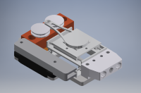
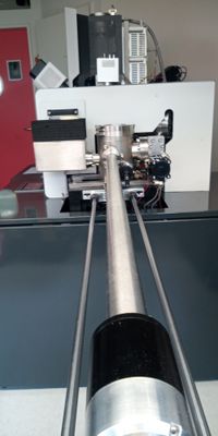
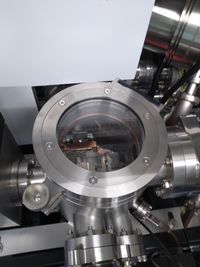
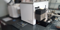
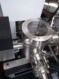
A small side chamber had to be developed and attached to an appropiate FIB port (mostly the Airlock-Port). The chamber is necessary to achieve the necessary UHV conditions for APT. The chamber is amongst other equipped with an MCP based Delay Line Detector (Diameter 80 mm), Cool Head, Hich Voltage Connectors, Laser Ports with associated manipulating optics and transfer mechanics.
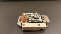
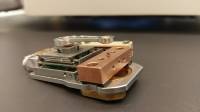
The sample of interest is mounted onto the shuttle
Transfer
- Transfer of the shuttle into the FIB chamber
- Localisation: The micro stage electrode is rotated backwards to open the view onto the sample. Localisation of the feature of interest
- Milling: a) The feature of interest is milled or prepared by Lift Out procedure b) the electrode is machined by the Ion Beam
- Positioning: The micro stage electrode is rotated back towards the sample. Using the SEM Beam, the electrode is positioned precisely above the the milled feature.
- Transfer into the M-Tap: The shuttle is transfered back into the side chamber.It is cooled down to croygenic temperatures and aligned relativ to the laser spot. APT measurement is started.
Samples are mounted directly onto the Shuttle. Using the transfer mechanics the complete shuttle can be transferred directly into the Dual Beam instrument. Allowing direct manipulation of the sample using Dual Beam Techniques.
Optional Airlock Chamber with Cryo Option
 | |
Optional Airlock-chamber with Cryo-Option | Pneumatic attachment of the Cooling Unit |
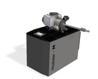
Specs: Orbis - Modular Atom Probe -
Modular Atom Probe + Sample Shuttle
OPTION
Cryo system
Optical System
Sample Stage
Vacuum system
Transfer Chamber / Airlock on request
Laser Options |
UV Nanochiplaser
| Picosecond industrial laser (10ps, 6W)
| Femtosecond Laser
|